

Glass PCBs Explained: Advantages, Limitations, and Real-World Us
发布时间:2026-07-08 17:17:31 分类:营销学堂
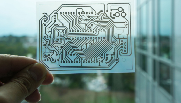 Glass is one of the several alternative materials used in PCBs as a base substrate instead of the more conventionally used materials like FR-4, Rogers, Polyimide, PTFE, etc. Glass has unique features, which makes it preferable where the application demands tough performance, reliability, and durability.
Glass PCBs are fabricated from a range of different glass materials and are tailored to meet specific application requirements. Some common types of glass used as a PCB substrate include:
- Borosilicate Glass: It provides a good combination of electrical, thermal and mechanical characteristics and has an operating temperature of up to 315°C.
- Aluminosilicate Glass: It has similar properties to borosilicate but with even lower dielectric loss, enabling higher frequency operation.
- Fused Silica Glass: It is an ultrapure glass made only from silicon dioxide and has the best thermal stability and the lowest thermal expansion of any glass material. This glass material can withstand temperatures of over 1000°C.
- E-Glass: It is an Aluminoborosilicate glass reinforced with glass fibers, giving it excellent mechanical strength while maintaining high heat resistance and stable electrical properties.
Structure of Glass PCBs
In glass PCBs, the glass core acts as the primary mechanical support, providing the required mechanical strength and dielectric for the board. On this glass core, a layer of copper foil is laminated, forming conductive paths to allow for electrical connectivity. Adhesive layers are used to bind the copper foil firmly onto the glass core ensuring stable and reliable connections. Protective solder masks or silkscreen coatings are added to the circuit board to protect it from environmental damage. It also helps in labeling the copper traces for accurate placement or identification of the electronic components on a given board.
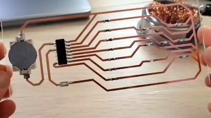
Glass PCB manufacturing uses sputtering, evaporation, or electroplating processes to deposit the various metal layers on the glass substrates. The desired circuit pattern is formed using lithography processes that involve applying a photoresist layer to etch the exposed metal on the substrate. This process can also be used to make a multilayer glass PCB where the various interconnections between the layers are created using vias or micro vias through a laser drilling process. The various active and passive components are assembled onto the glass PCB by soldering or using conductive adhesives.
Advantages of Glass PCB Substrates
- Thermal Stability: Glass substrates have very low coefficients of thermal expansion and high thermal stability providing excellent pathways for dissipation and greater board stability, guaranteeing long-term reliability and durability in even the most critical of applications.
- High-Frequency Performance: They have very stable dielectric properties that are responsible for low dielectric loss and interference even at high frequencies.
- Mechanical & Chemical Resistance: Glass has very high flexural strength and is highly resistant to cracks and fractures. It also has superior chemical resistance and does not absorb moisture like other conventional substrate materials like FR-4. This improves the reliability and lifespan of Glass PCBs and makes them suitable for demanding structural applications.
Limitations of Glass Substrates
The major limitation of using glass is its fragility, which makes it difficult to handle and manage. The size of the glass PCB increases this disadvantage even more as larger glass panels are even more prone to damage. The size factor renders them less useful in larger applications, as they are ideal only for small and confined applications.
Applications of Glass PCB Substrates
- LED & Displays: The transparency properties of glass make it ideal for use in applications like LED lighting and various interactive display technologies.
- High-Speed Digital Circuits: Glass PCBs can support high-speed digital circuits used in compute, telecom, automotive and medical applications operating at multi-GHz frequencies.
- Antennas: The stable dielectric properties of glass at mmWave frequencies are also ideal for antenna applications.
- Power Electronics: Glass handles thermal conductivity at high power densities more efficiently which is useful for power electronics. Being able to operate at over 200°C continuously makes them suitable for downhole, aerospace and automotive applications.
- Medical Implants: The durability and biological inertness of glass allow it to be used in implantable devices for medical applications.
- Harsh Environment Sensors: Resistant to corrosion and humidity, glass PCBs are widely used for sensors and transducers that operate in harsh environment sensors.